![]()
In the previous article, we talked about "How to Increase the bonding force for PCBA by using "Copper" base as the PCB surface finish“. Today, we will discuss further how the SMD (Solder Mask Defined) and NSMD (Non-Solder Mask Defined) pad designs of the BGA package affect the solderability and how these two types of pads affect the bonding force of PCA.
Increasing the solder contact area of a component terminal or leads will generally improve the solderability of the component, as it provides more surface area for the solder to wet and bond to the terminal. This can result in a stronger and more reliable solder joint.
However, it’s important to note that there are other factors that can also affect solderability, such as the type of surface finish on the component terminal and the solderability of the solder itself. So while increasing the solder contact area can be beneficial, it may not be the only factor to consider when trying to improve the solderability of a component.
II. Increasing the solder contact area of the component’s terminals or leads
Please note: what I mentioned here is to increase the contact area of the component’s solder terminals or leads, not to increase the amount volume of solder.
Before reading this article, it is recommended that you refer to the article of "Concept Clarification of Electronic Component Soldering Strength" by workingbear first.
Workingbear must emphasize again: "The soldering strength is basically proportional to the soldering contact area". Without considering the replacement of the solder paste formula and the surface finishes of the PCB (Printed Circuit Board), there are two key points to enhance the soldering strength of the component:
1. Increasing the solder contact area of the component’s terminals or leads. It’s not the amount volume!
If only more solder is added to the solder balls of the BGA, its solder strength will not increase basically, because its solder pad contact area remains the same. For SMD components with leads (such as QFP) or side solder terminals (such as the capacitor), increasing the amount volume of solder may increase its solder strength, because the leads of these SMD components have side terminals that may have solder climb up to higher position and increase the solder contact area.
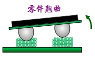
If the solder amount can be increased to allow the solder to form a complete curve on the side of the solder foot, the solder strength can be effectively increased. Just like adding a support on the side of a tree or a utility pole to prevent it from falling down in the event of a typhoon, adding an R angle at the corner of a mechanism design is also the same principle, and the arc-shaped solder can effectively disperse stress.
Therefore, if increasing the amount of solder can allow the solder to climb up the sides of the solder terminals or leads, and even make the side solder climb higher to completely cover the solder leads, then its strength will increase significantly. This is much better than just welding at the bottom of the solder leads because you have increased the soldering area and its soldering structure has been strengthened.
Unfortunately, the side walls of most SMD component leads are not electroplated directly on bare copper due to cost considerations, which causes them to easily oxidize and cannot be soldered. Otherwise, they are electroplated, but the pitch between the lead is too small, causing the design of the PCB solder pad to be afraid of short-circuits and unable to extend so that the solder cannot completely climb up its side to form a perfect arc.
![]()
![]()
Since climbing solder on the side walls of the solder lead can increase the solder contact area and strength, many people focus on the grounding foot (GND), such as increasing the circular or semi-circular holes on the ground pin of the B2B connector at both ends or designing it into a "U" shape, which all have the opportunity to increase its solder strength.
Since we’re talking about how increasing the soldering contact area can help to enhance the strength of the solder, we have to briefly mention the pros and cons of SMD and NSMD pad designs for BGA packaging on the PCB side.
Please note that we should not confuse the "SMD (Solder Mask Defined) pad" with the "SMD (Surface Mount Device) component" here.
![]()
Assuming that the exposed area of SMD and NSMD pad designs is the same, the solderability of NSMD pads should be better than that of SMD pads. As mentioned earlier, this is because NSMD pads will wet the side walls of the pads during soldering, while SMD pads do not have side walls due to being covered by the solder mask. (NSMD is also called "Copper Defined pad.")
But don’t rush to change all BGA pads to NSMD designs immediately because there is no perfect solution if BGA cracking! In this fair world, even if the exposed pad surface of SMD and NSMD seems to have the same size, the actual size of the SMD pad is much larger than that of NSMD (depending on the layout design). This is because a large part of the SMD pad is covered by the green solder mask actually, and it is easy to be deceived if you don’t look carefully. Because the size of NSMD pads is relatively small, almost only slightly larger than the solder balls of BGA, the ability of SMD pads to withstand pulling force will be relatively poor. Once the BGA solder ball breaks, it is often seen that the NSMD pads are pulled up together with the solder balls.
As mentioned by the workingbear before, stress will find the weakest point to release. When the pad changes from NSMD to SMD and the soldering strength increases, the ability of the solder IMC layer to resist stress becomes greater than the bonding force of the PCB copper foil attached to the substrate (because the size of the SMD pad becomes smaller), and the breaking point shifts to between the pad and the FR4 substrate. Therefore, the workingbear still believes that if you want to completely solve the problem of BGA cracking, you should try to reduce stress, which is the only way to achieve the best improvement.
Therefore, the conclusion is that NSMD pads have better solderability than SMD pads, while the bonding strength of SMD pads is better than that of NSMD pads.
2.Using Through-Hole component to Replace Surface Mount device
In fact, no matter how much the solder strength of electronic components using surface mount technology (SMT) is improved, its ability to resist stress is limited. To further increase the strength of the solder, the stress needs to be transmitted to other structures through mechanism design. The most effective way to achieve this is to design the pins as upright plated through-holes (PTHs), so that the stress on the pins can be transferred to the hole walls of the printed circuit board (PCB) for support, which in turn can increase the strength of the solder. The common practice is to change some of the surface-mount soldering of the component pins to through-hole soldering, such as the iron frame soldering pins of Micro-USB connectors. They still go through the SMT process, but some of the pins are produced using the paste-in-hole (PIH) process. The latest Type-C connectors also have parts with a mix of through-hole and surface-mount soldering.
In addition, for ball grid array (BGA) packaged components, we can consider to layout vias on the pads, just like a rivet to fix the pad on the FR4 material. This is similar to the idea of anchoring a house with ground screws to prevent seismic damage. However, the vias on the solder pads must be electroplated and filled, otherwise, the BGA’s solder balls may form voids or bubbles, which can lead to severe defects, such as the head-in-pillow effect.
Recommended reading: Principles of via-in-pad handling.
Article series :
Related article:
Increase solder paste volume will improve the MLCC capacitor broken?
The post
Why BGA soldering ball always crack(5)? Increase the contact area of solder to increase its strength first appeared on
電子製造,工作狂人(ResearchMFG).
 < 2sec】。")

 不過工作熊個人建議,不只要管控錫球的「融錫時間差(LTD)」,更要順便管控其「固化時間差(STD, Solidus Time Delay)」,其實只要稍加注意調整回焊爐溫度的設定條件兩者就可以同時得到改善,何樂不為。
與HIP(Head-In-Pillow)或HoP(Head-of-Pillow)在SMT的Reflow溫度曲線下形成的原因稍微做了解釋,基本上兩者都是因為板材變形所致,只是HIP的錫膏會保留在電路板的焊墊上,但NWO則完全轉移到了錫球。")


對各種焊接不良的影響與效果")
") 「錫珠」也稱「焊珠」是相當常見的焊錫缺陷之一,它經常出現在零件本體的下方,尤其是在小電阻、小電容等small-chip本體下兩個端點的中間側面。
「錫珠」也稱「焊珠」是相當常見的焊錫缺陷之一,它經常出現在零件本體的下方,尤其是在小電阻、小電容等small-chip本體下兩個端點的中間側面。")
")
")
")
") 墓碑效應(Tombstone)是因為同一個零件兩端融錫時間不一致,最終造成兩端受力不均,以致一端受力較大為支點舉起零件另一端懸空而成。
墓碑效應(Tombstone)是因為同一個零件兩端融錫時間不一致,最終造成兩端受力不均,以致一端受力較大為支點舉起零件另一端懸空而成。

 最後,提醒電路及電路板設計者們一件事,SMT工廠為了避免錫膏在大焊墊的融錫過程中因內聚力而群聚至某一區域而導致零件頂高,造成零件傾斜,最後形成單側吃錫不良之現象,會在開EPad鋼板時做井字形、田字行、米字形或條紋形狀的開孔,其錫膏覆蓋率大概只會有EPad面積的50~60%,如果PCB的散熱墊(thermal pad)上又有過多未塞孔電鍍的導通孔(vias),為了避免錫膏流入到這些vias造成錫量不足以及溢流對板子另一面造成錫珠或短路等問題,在錫膏印刷時都會特意避開這些vias,這可能使得EPad焊接的氣泡空洞率增加大於50%,甚至來到70%的空洞率,那就可能使得熱阻增加、熱導率降低並影響到散熱的效果。


之工藝")


 這是因為錫膏中含有助焊劑,而助焊劑中又含有乙醇類等易揮發的溶劑,也就是說錫膏一旦開封後溶劑就會開始揮發(其實不開蓋密封的情況下也會揮發,只是速度很慢,就類似汽水裝在寶特瓶中一段時間後也會沒氣是一樣的道理),尤其是那些已經塗抹在鋼板或是已印刷在PCB上的錫膏,其溶劑揮發的速度會更快,所以,一般有紀律的SMT廠都會嚴格管控錫膏的使用標準及壽命。


")


 其三,錫膏開罐後暴露於生產車間的時間又是如何管控的?我們前面已經說過,錫膏開罐後,錫膏中的溶劑就會開始揮發,所以我們不只要管控錫膏直接暴露於大氣環境下的溼度,更要管控暴露的時間,因為暴露時間越長,溶劑的揮發就越多,出問題的機率也就越高。一般我們會要求錫膏開蓋超過8H不得回收,超過12H或24H報廢,不建議自己添加溶劑,因為你不知道溶劑揮發了多少,更不知道需要添加多少溶劑,添加了溶劑後還得重新充分攪拌均勻。而對於已經塗抹於鋼板上的錫膏,其溶劑揮發的速度會比在罐子裡的更快,一般建議要在3H內用完。


 利用添加劑的特性,控制局部區域銅的生長速率,來進行填孔的目的,只是電鍍填孔的孔徑不可太大,一般只能在使用雷射鑽孔的微通孔(micro-via)中使用。電鍍塞孔有樹脂塞孔後電鍍的所有優點,但是不會有空氣藏在通孔中的問題,缺點是價格較貴,且填孔後容易出現表面凹陷的dimple,dimple如果太深。容易造成BGA空焊及孔洞問題,所以需要與PCB製造商訂定dimple深度的規格。


